
Modern electronics use printed circuit boards to connect components. These boards, often made of flame-retardant FR-4 fibreglass, are key in devices like smartphones and medical gear. They replace messy wiring with copper layers etched into patterns, making devices more efficient and smaller.
Boards are made to different standards. Class 1 boards are for simple items like remote controls. Class 2 boards are for industrial machines that last longer. And Class 3 boards are for critical systems in aerospace or pacemakers, needing to work perfectly under harsh conditions.
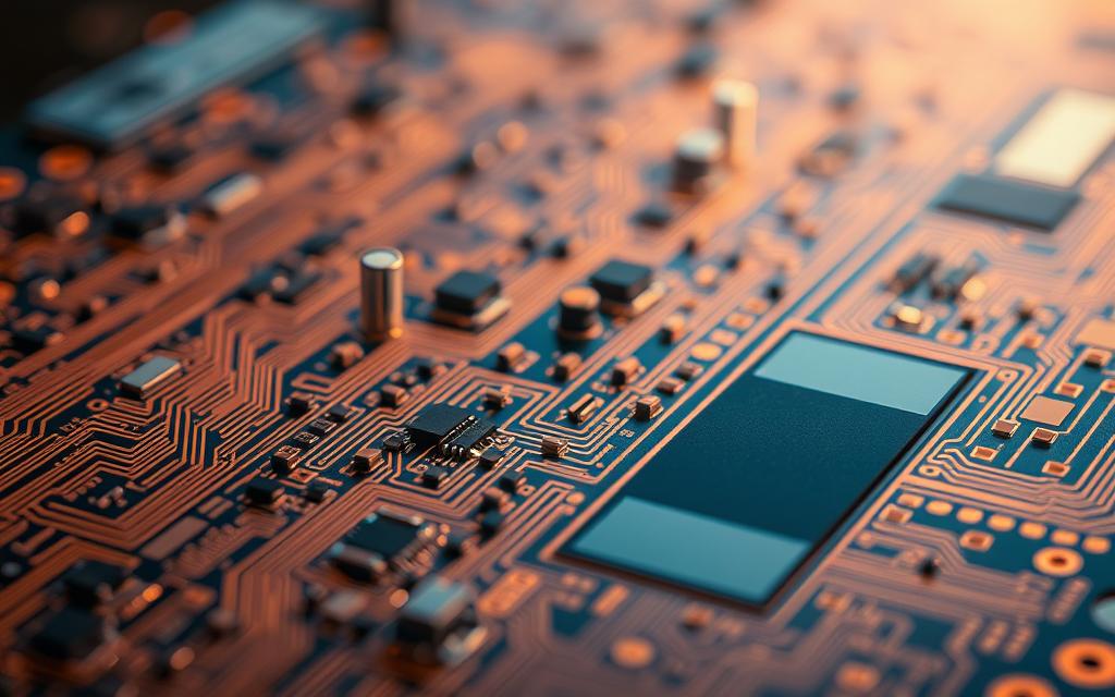
Looking at pcb basics printed alongside fast growing tracking pace gives a clearer view of the wider topic.
Looking at pcb basics printed alongside cyclonic grilling gives a clearer view of the wider topic.
The way PCB fundamentals have evolved has changed how devices are made smaller. Modern boards have layers for complex circuits and features to keep them cool. Engineers use special materials for 5G networks, showing how important these boards are for new technology.
The Evolution of Circuit Board Design
The journey from simple electrical systems to today’s advanced PCBs shows how engineering has changed electronics. This change didn’t happen quickly. It was a series of small steps, driven by military needs, industrial demands, and what people wanted.
From Point-to-Point Wiring to Modern PCBs
Early 20th century electrical connections
Before PCBs, people used to solder wire labyrinths by hand to connect devices like radios. These setups were often fragile and prone to failure. A 1925 telephone switchboard had over 900 metres of wiring, showing how inefficient early connections were.
World War II was a turning point. The need for compact, reliable circuits in artillery shells led to changes. By 1948, the US military had standardised printed wiring. This made making circuits 75% faster than before. This change helped consumer electronics grow in the 1950s.
Related Posts:
- What Is IO in Technology Understanding Input Output Systems

- What Is DWDM Technology Dense Wavelength Division…

- How Technology Is Changing Business Communication…

- What is cyclonic grilling technology?

- What Is CSP Technology An Overview of Communication…

- How Technology Affected Globalization Connecting the World

Key Milestones in PCB Development
1943: Paul Eisler’s printed wiring patent
The Austrian inventor Paul Eisler created an etching technique on copper-clad boards. His patent was initially overlooked but later became key for mass-producing circuits. His 1957 BBC television set prototype showed the idea’s worth in the market.
1956: US Army’s automated assembly processes
The US Army’s work on automation led to big improvements. The Auto-Sembly system could make 500 boards an hour. This made electronics cheaper for the public.
1980s: Surface-mount technology revolution
SMT components got rid of wire leads, making smaller circuit boards with more components. The first SMT Walkman (1982) showed how much more could be done in less space than before.
What Is PCB Technology?
Printed circuit board technology is at the core of today’s electronics. It’s the base of everything from smartphones to big machines. It makes sure components can talk to each other well. Let’s dive into what PCB technology is and why it’s key in today’s engineering.

Core Definition and Function
Electrical Interconnection Platform Definition
A printed circuit board is a structured base for electronic components. It’s different from old wiring methods. PCBs have special paths called traces etched on insulators. This makes connections neat and reliable.
Current Conduction vs Signal Routing Functions
PCB traces have two main jobs. Current conduction is for power, using thick copper paths. Signal routing is for data, using thin traces. This is key for devices like Wi-Fi routers.
Fundamental PCB Characteristics
Multi-Layer Construction Principles
Complex devices use multi-layer PCB construction. They have 4 to 12+ layers stacked. Server motherboards are a great example, with layers for power, ground, and signals. Vias, tiny holes, connect layers without interference.
Standardised Copper Thickness Measurements
Copper thickness affects how much current a PCB can handle. Here are some common standards:
- 1 oz/sq ft (35 µm): Low-power devices
- 2 oz/sq ft (70 µm): Cars and control units
- 3 oz/sq ft (105 µm): Heavy-duty equipment
Dielectric Material Properties
The insulating substrate’s dielectric materials are very important. FR-4 fibreglass is used in most PCBs. It has:
| Property | Value | Significance |
|---|---|---|
| Thermal Resistance | 130–140°C | Prevents warping during soldering |
| Dielectric Constant | 4.3–4.9 | Maintains signal speed |
| Flame Retardancy | UL94 V-0 Rating | Meets safety standards |
For high-speed needs, like 5G, special substrates like Rogers 4350B are used. They help keep signals strong.
Essential PCB Components and Materials
Modern printed circuit boards use special materials and components. They need to be strong, conductive, and easy to make. This section looks at the key parts that make up a PCB.
Base Structural Elements
The base of any PCB is its substrate and conductive layers. The choice of material affects how flexible, heat-resistant, and good at carrying signals it is.
Substrate materials: FR-4 vs polyimide
FR-4 is the go-to for rigid boards. It’s strong and doesn’t catch fire easily. It’s perfect for most gadgets. Polyimide is used for flexible circuits. It can handle very high temperatures, making it great for cars and planes.
| Property | FR-4 | Polyimide |
|---|---|---|
| Flexibility | Rigid | Flexible |
| Max Temp | 130°C | 260°C |
| Cost | £ | £££ |
Copper foil types and weights
Electrodeposited copper (ED) makes fine traces smooth. Rolled-annealed (RA) foil is more flexible. Common weights are:
- ½ oz (18µm) for high-density designs
- 1 oz (35µm) for standard power handling
- 2 oz (70µm) in high-current applications
Critical Functional Layers
Specialised layers are needed for precise electrical performance and protection.
Conductive pathways etching process
Photolithography creates circuit patterns by:
- Applying UV-sensitive photoresist
- Exposing through a patterned mask
- Chemical etching of unwanted copper
Solder mask composition and colour variations
Epoxy-based solder masks stop short circuits and let soldering happen. Green is common, but modern boards use:
- Red for high-visibility prototypes
- Blue in gaming hardware
- Black in premium consumer devices
Silkscreen labelling requirements
White epoxy ink marks components and shows polarity. Standards require:
- Legible text ≥0.8mm height
- Clear polarity indicators
- Reference designators matching schematics
Advanced Component Integration
Modern electronics need new ways to mount complex parts.
Through-hole vs surface-mount components
Through-hole technology (THT) is good for repairs and reliability. Surface-mount devices (SMD) fit automated assembly of small designs.
Ball grid array (BGA) packaging
BGA packaging uses solder balls under chips. It increases pin density by 50% over QFP packages. This is key for modern chips and FPGAs.
High-density interconnect (HDI) features
HDI PCBs use microvias and buried traces. They’re great for 5G routers and wearable tech. Key features include:
- Blind/buried vias ≤150µm diameter
- Stacked via configurations
- Thin dielectric layers (≤50µm)
PCB Manufacturing Process Breakdown
Modern PCB making uses precise engineering and strict quality checks. It turns digital designs into working circuit boards. This process has three main steps, each needing special skills and the latest tech.

Design and Prototyping Phase
Designers start with CAD software like OrCAD or Altium Designer. They make detailed diagrams. These tools help place components correctly and check electrical rules.
Design for Manufacturability (DFM) Checks
DFM checks spot problems before making prototypes. They look at:
- Minimum trace width verification
- Drill hole alignment tolerances
- Copper weight distribution analysis
Industrial Production Stages
After designs are checked, manufacturers start the production process. This needs very precise work.
Photolithography Process Steps
This method transfers patterns onto the board through chemical reactions:
| Stage | Process | Purpose |
|---|---|---|
| 1. Cleaning | Alkaline solution bath | Remove surface contaminants |
| 2. Lamination | Dry film resist application | Create UV-sensitive layer |
| 3. Exposure | UV light through photomask | Transfer circuit pattern |
Chemical Etching Precision Controls
Ferric chloride solutions remove copper with up to ±0.025mm accuracy. The etching baths are kept at 45-55°C for best results.
Automated Optical Inspection (AOI) Systems
High-resolution cameras check boards for defects like:
- Incomplete traces
- Solder mask irregularities
- Component misalignment
Quality Assurance Protocols
Final checks make sure boards work well in different fields.
IPC-A-600 Acceptance Criteria
This global standard sets rules for:
- Solder joint integrity
- Conductor spacing
- Substrate delamination resistance
Environmental Stress Testing Methods
Aerospace-grade boards face 500+ thermal cycles. This checks how they perform in extreme temperatures.
Cross-Section Analysis Techniques
Microscopic checks look at plated through-holes for:
- Copper distribution uniformity
- Interconnect voiding
- Layer alignment accuracy
Contemporary Applications and Future Directions
Printed circuit boards are changing fast, meeting today’s needs and looking to the future. They help us connect quickly and power important medical devices. This shows how versatile PCBs are in many areas.
Current Industry Implementations
Three main areas are pushing PCB technology forward with their unique needs:
5G network infrastructure demands
5G PCBs use special materials to handle fast data. They help base stations work better, making data speeds very high.
Electric vehicle power systems
PCBs in EVs manage battery health. They can handle lots of cells and tough conditions.
Medical imaging equipment requirements
MRI machines use special PCBs to avoid interference. This helps find small tumours.
Emerging Technological Frontiers
New ways are changing how PCBs are made:
3D-printed electronics integration
A new method prints antennas on curved surfaces. It makes IoT devices smaller and simpler.
Biodegradable substrate research
Scientists at Cambridge are working on biodegradable substrates. These boards break down in soil, helping reduce waste.
AI-optimised design trends
AI helps design PCBs for data centres. It makes them better and more efficient.
These changes are part of a bigger move towards green electronics. Our look at smart home PCBs shows how important this is. It’s a big step forward for the next decade.
Conclusion
Printed circuit boards are key to modern tech progress. They power everything from Apple’s smartphones to Tesla’s electric cars. They also help in making life-saving medical gear like MRI scanners and defibrillators.
PCBs are vital in new energy systems and space tech. SpaceX uses them for satellite and rocket control. As IoT and 5G grow, PCBs will keep playing a big role.
Now, making PCBs must be green. Samsung and Panasonic use eco-friendly materials and methods. AI helps make production better, cutting down waste and improving accuracy.
Engineers need to know PCB basics for new tech challenges. This includes better cooling and signal quality. As tech gets more complex, knowing PCBs is key.
PCB tech links ideas to reality. It’s used in everything from Arduino projects to Siemens automation. Its growth will help create smarter cities and better healthcare and energy systems.
FAQ
What distinguishes Class 1, 2, and 3 PCBs in industrial applications?
Class 1 PCBs are for simple electronics like LED lights. Class 2 boards are for industrial gear, like HVAC systems, needing more strength. Class 3 PCBs are for top-notch uses in aerospace or medicine, like pacemakers or satellites.
How does copper weight affect a PCB’s functionality?
Copper weight affects how much current a PCB can carry and its heat management. Thicker copper (2–3 oz) is for high-power needs in cars. Thinner copper (½ oz) is for low-current needs in gadgets like earphones.
Why did surface-mount technology replace through-hole components in the 1980s?
Surface-mount technology (SMT) made assembly easier and boards smaller by avoiding holes. This led to devices like Sony Walkmans, where components were soldered directly onto pads.
What are the advantages of using FR-4 over polyimide substrates?
FR-4 is rigid, affordable, and fire-resistant for common uses like router boards. Polyimide is for extreme conditions, like in foldable phones or Mars rovers, due to its flexibility and heat resistance.
How do military standards influence modern PCB manufacturing?
WWII innovations led to strong, mass-made boards. The US Army’s automation and IPC-A-600 standards for solder quality are key, ensuring aerospace PCBs pass tests from -55°C to 125°C.
What role does photolithography play in PCB fabrication?
Photolithography uses UV light and chemicals to create circuit patterns on boards. It’s vital for making tiny traces in devices like iPhone logic boards, unlike manual etching.
Why are high-frequency materials like Rogers 4350B used in 5G base station PCBs?
These materials reduce signal loss at high frequencies, keeping 5G speeds up. FR-4 would cause signal loss in routers handling big data speeds.
How are BGAs and HDI technologies enabling advanced electronics?
Ball grid arrays (BGAs) enable tight connections for chips like AMD Ryzen. High-density interconnect (HDI) PCBs use tiny spaces for signals in small devices, like 5G phones and implants.
What environmental innovations are emerging in PCB production?
New substrates from plants like flax or hemp are being explored to cut down on waste. Companies like IBM are testing packaging from mushrooms. The EU is pushing for non-toxic solder masks.
How do AI tools enhance PCB design processes?
AI software like Cadence Cerebrus optimises component placement in server boards. It analyses thousands of layouts an hour, a task too big for humans.